25.11.2022 - Osprey
I have been struggling to learn proper touch-typing for a long time. My ugly 6-finger-technique is simply faster than I can touch-type so I always fall back into typing "wrongly" and never get enough practice into it to actually improve. That's why I have been eyeing the ergo scene for a while now - no way to type in any but the proper way on a column stagger ergo board. A friend of mine then showed me the REVIUNG41, and we decided to base our own board on its stagger, but change a lot of other things. This started out as a quick and easy design project, then feature creep happened, then I was unsatisfied and re-did the whole PCB (twice), and it evolved into a one-year-design-project.
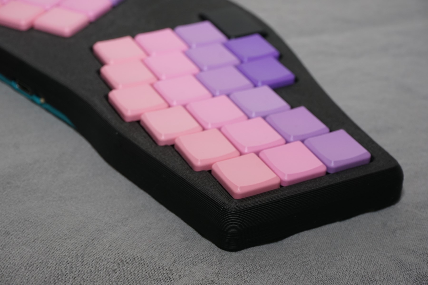
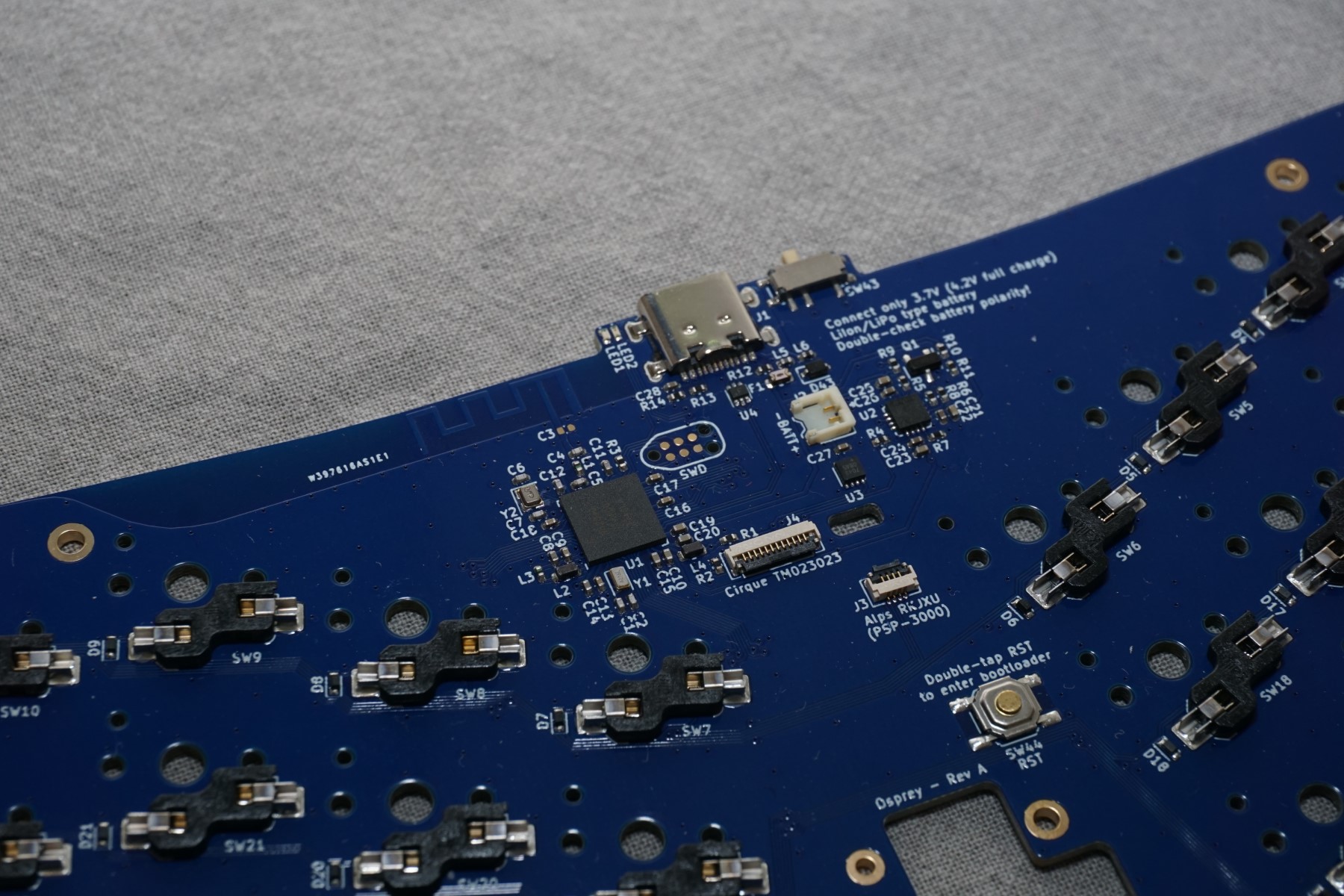
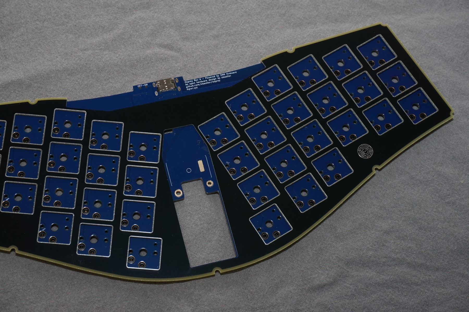
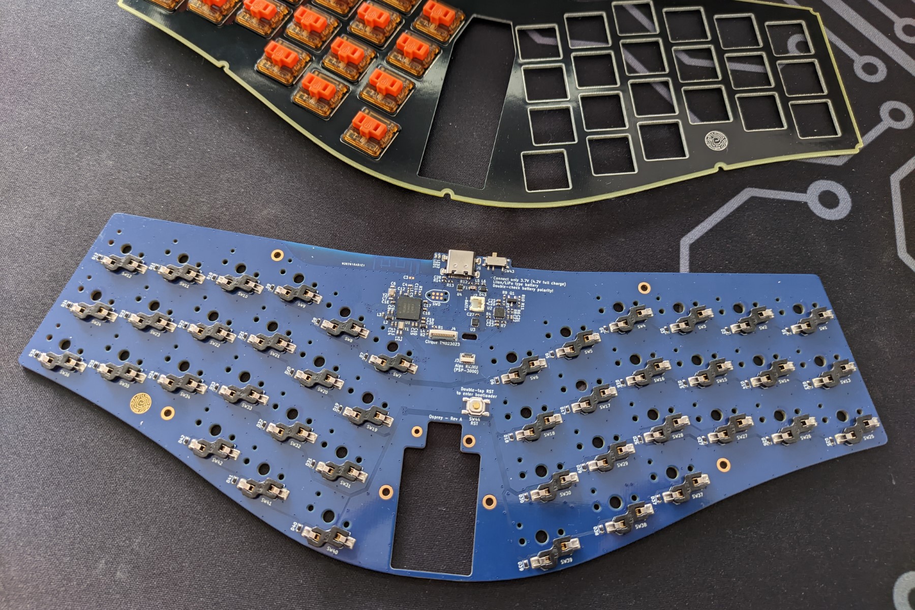
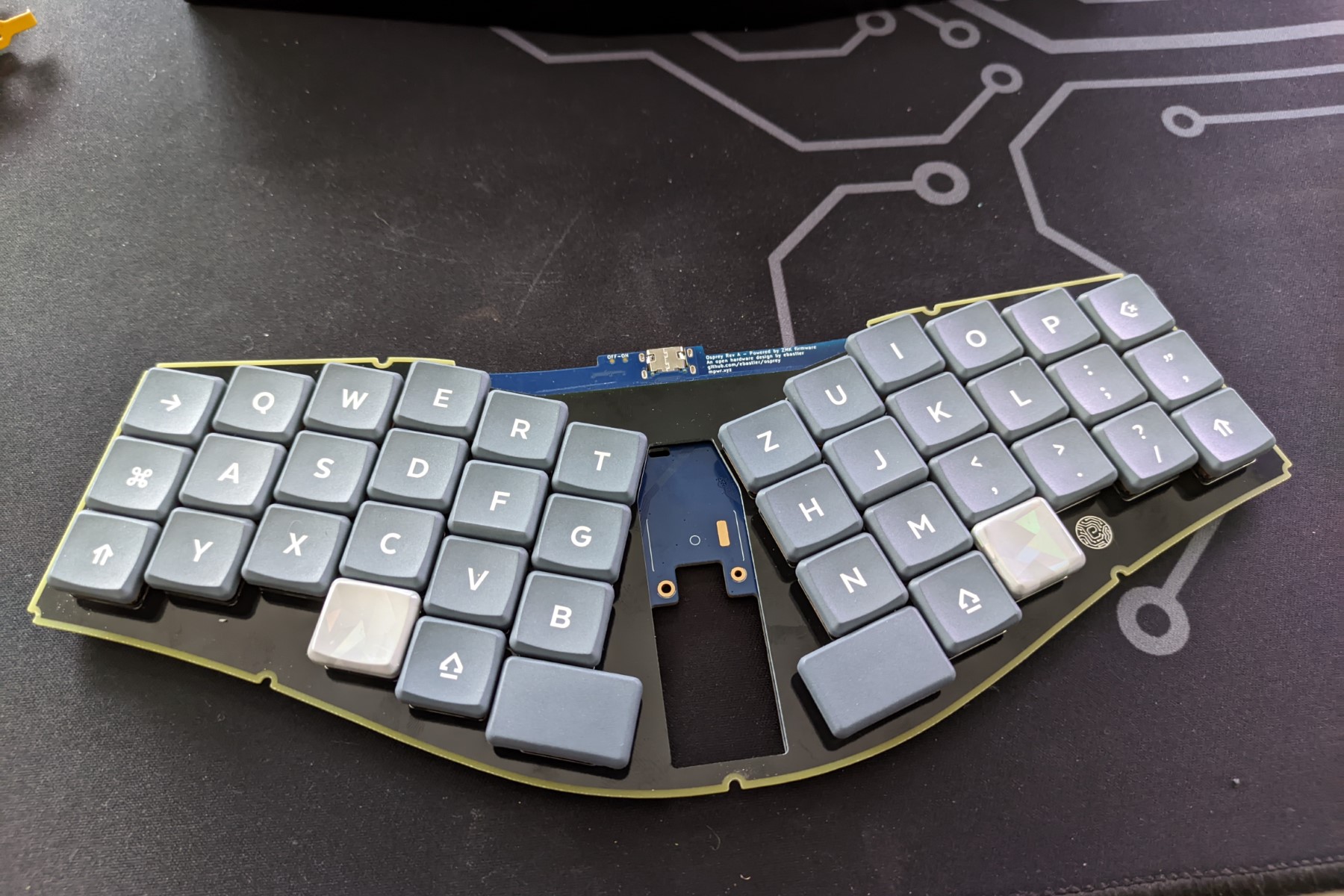
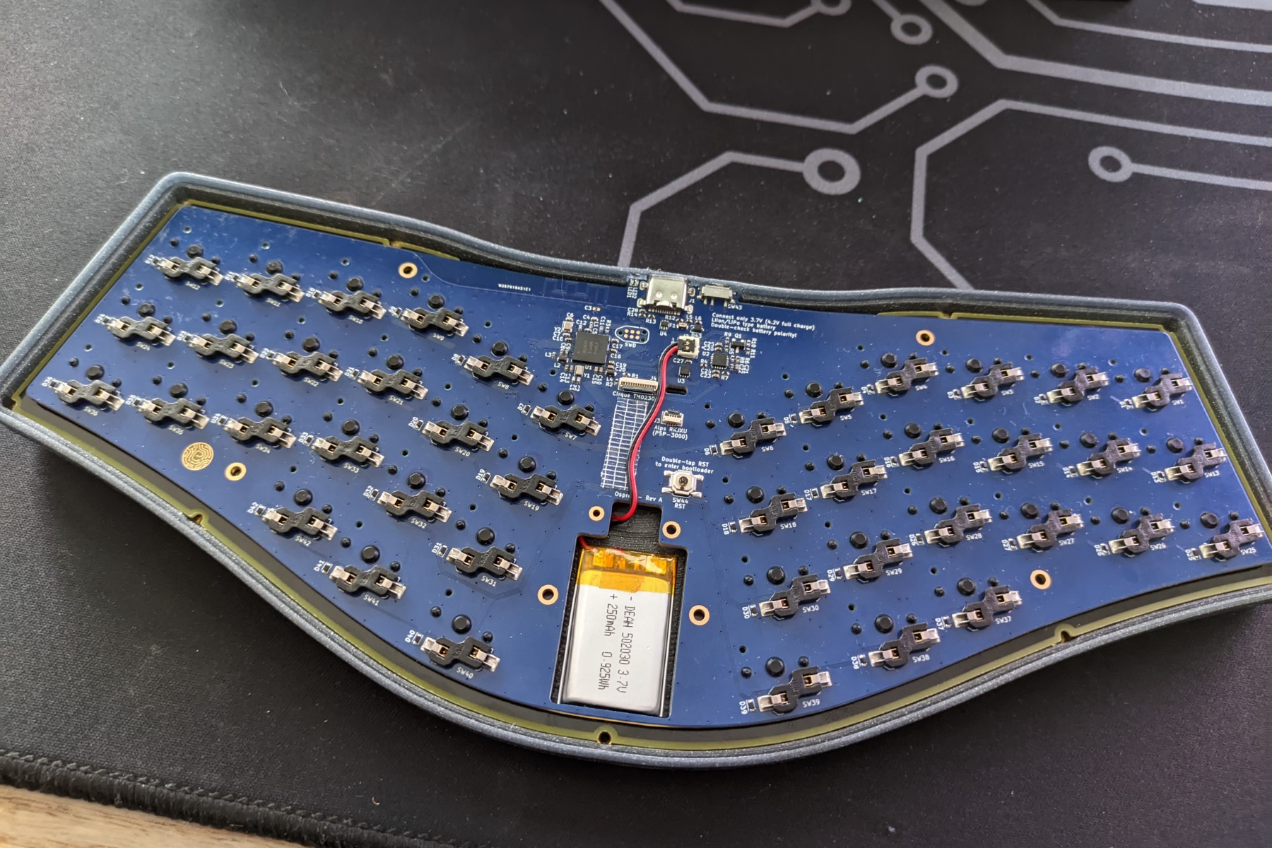
The final design uses a similar stagger as the Reviung, but the halves feature a steeper angle between each other, the thumb cluster was changed to three keys per hand, and we switched to Kailh Choc switch spacing (as it is Choc v1 only). Electronics-wise it uses a bare nRF52840 chip directly on the PCB, paired with a Texas Instruments BQ24075 battery charging/Powerpath chip, and a Maxim MAX17048 fuel gauge. We also added support for either an Alps RKJXU (better known as PSP-3000 thumbstick), or a Cirque TMO23023 23 mm touchpad in the center between the two keyclusters. ZMK, the open-source wireless-first keyboard firmware we opted to use, does not support them, and the case has no place to mount them yet, but both are work in progress, and support will follow eventually - the PCB will be ready.
Since the MCU is basically BGA (even if the package is called "aQFN") in order to reach all pins one would need plugged vias and/or microvias and a four layer PCB, but luckily I still had plenty of IO available using just the easily reachable outer pin row. For maximum battery life I decided to follow nordic sample schematic 4, which makes use of both DC-DC converter stages of the chip. The first stage will convert battery voltage to 3.3 V IO voltage, the second stage converts the 3.3 V IO voltage to 1.8 V for the core. It also features both crystals, allowing the board to disable the HS crystal for lower idle draw. Nordics example antenna matching matches to 50 Ohms of impedance, so I decided to use the antenna from Texas Instruments AN043, which already exists as a default library footprint in KiCAD, dimensioned for a 2 layer 1.6 mm PCB - exactly the stackup I was planning to use.
The chip would be designed for a 4 layer stackup, and needs a solid and unbroken RF ground. This is usually realized with a dedicated ground plane which I obviously could not make use of on 2 layers. Therefore I tried to keep all traces around the MCU on the top layer as much as possible, allowing for a single, unbroken ground plane spanning from the antenna, past the MCU, until the MCU decoupling capacitors. The routing took me a few iterations, and I used the reference layout as an orientation, even if my design was different from it due to the reduced layer count.
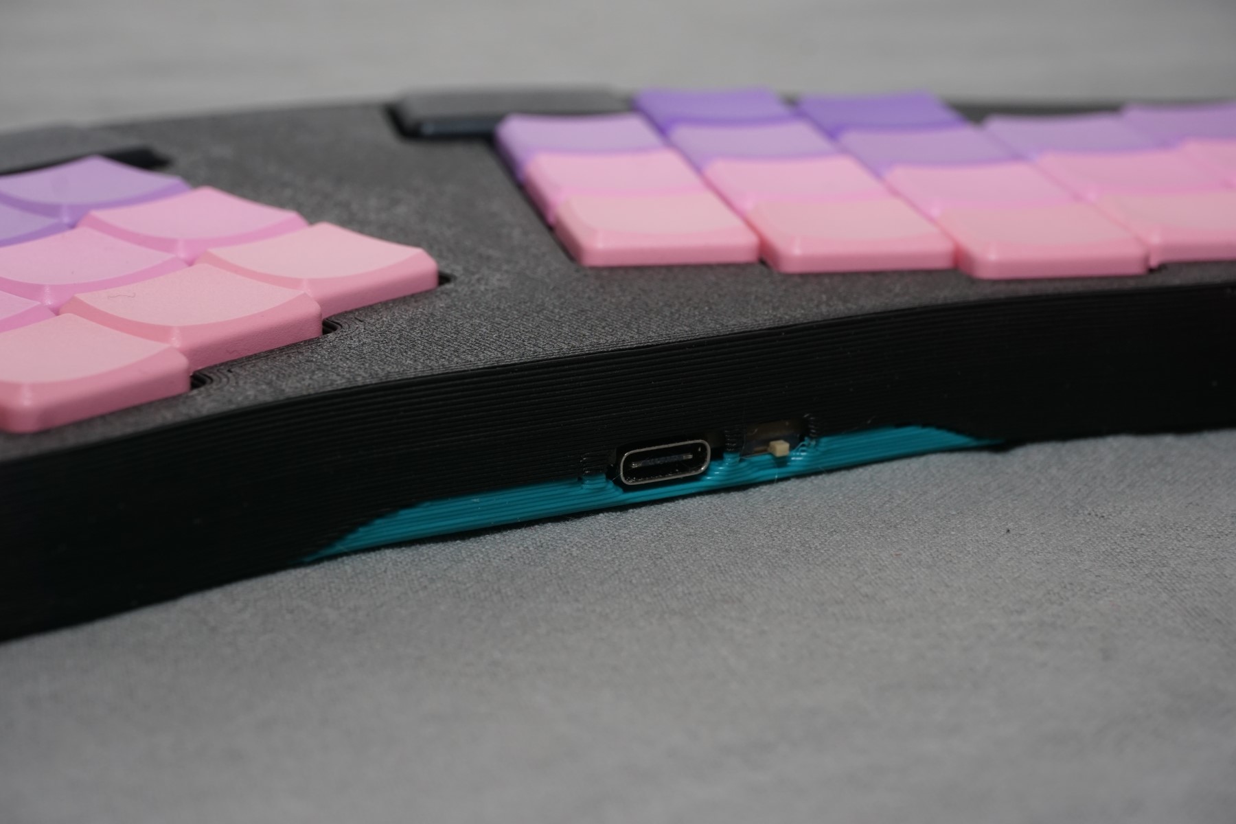
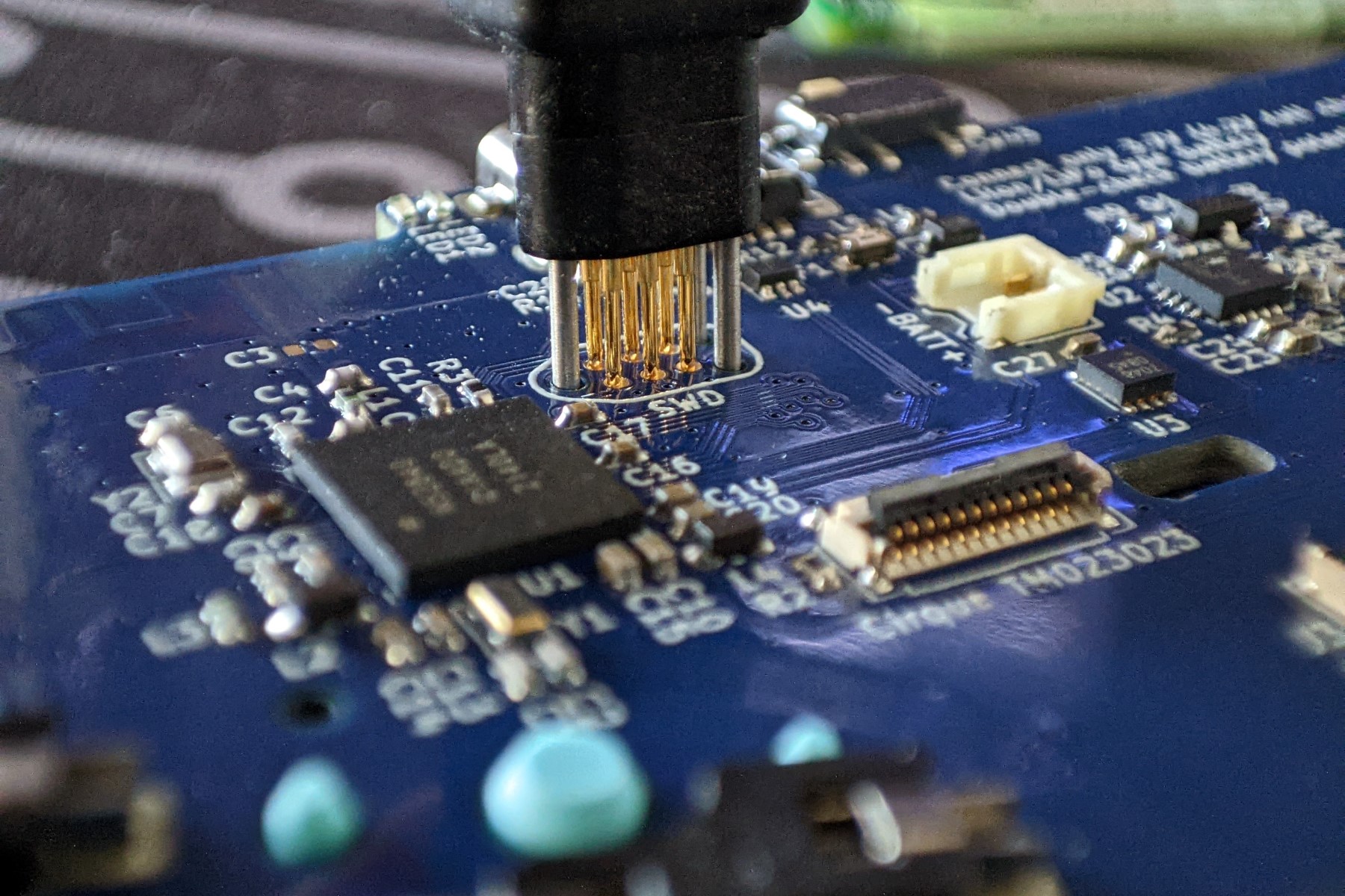
Everything else was quite straightforward - the USB-C port was fitted with with some filtering and ESD protections. I added a switch to the SYSOFF feature of the BQ24075, as that would allow to turn the board on and off, and an additional n-ch MOSFET. This one pulls SYSOFF low if VBUS is high to ensure that the board will always enable the battery when plugged in, regardless of the switch position. This is - in my opinion - essential, as most simpler designs can not charge while the switch is in OFF position. Since I expect the board to have a runtime of at least 2-3 months, charging is not a main concern, but still nice to do it properly. A TC2030 connector can be used for easy flashing, as nRF52840 are sold without any kind of bootloader, and need a hardware flashing tool to get them working once - afterwards the Adafruit UF2 Bootloader allows for easy updating of the firmware.
With the PCBs ready to order I had to tackle the cost of prototyping which would have been quite steep, around 75$ per PCB for a MOQ of five boards. Luckily PCBWay, a major PCB fabrication company and popular with hobbyists around the world, offered me a sponsored production run. They would take over the entire PCB cost in return for some exposure on social media. Ordering with them was a pleasant experience - basically one uploads the gerber files and BOM/POS files (you can find all of them in my Osprey git repo if you want to see an example), and their technicians would report back to me with questions that arose. They asked whether some hard to source components can be substituted with easier available ones (making the production faster and cheaper) and noticed some minor issues where my early BOM file was not clear or contained mistakes. Once we had all questions resolved, I could head on to the payment and they'd start sourcing all components. While they already had most components stocked, some more rare chips or passives needed to be ordered from suppliers. This was all done without requiring any interaction from my side, and quicker than I had anticipated. Once everything was ready for assembly, PCBWay sent me pictures of a single assembled PCB so I had a chance of double-checking component orientations before the final assembly. All of them were correctly placed, but it is nice being able to do a final check-up yourself, and not having to blindly trust a company, especially for larger orders worth hundreds or thousands of dollars.
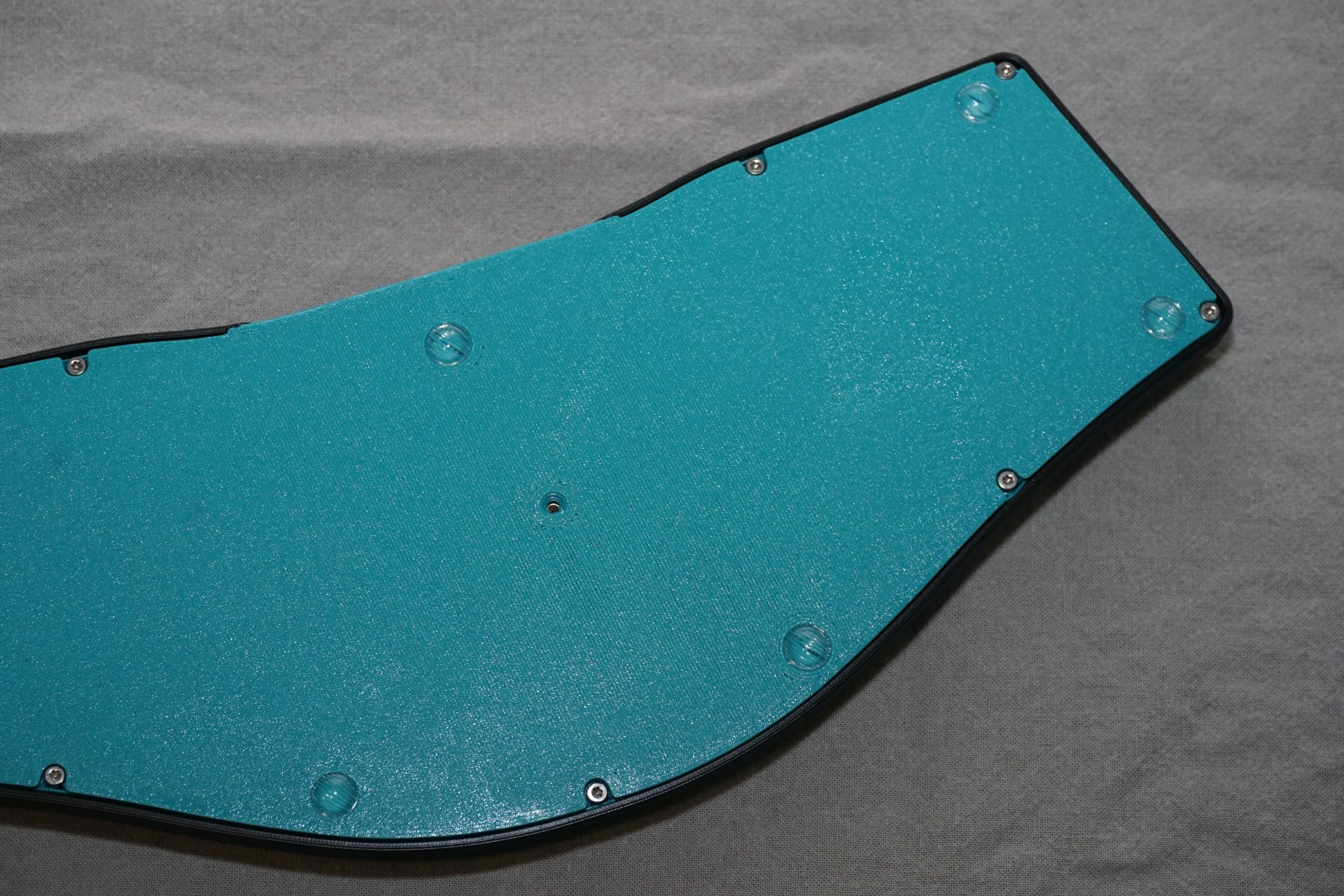
Last but not least - every keyboard needs an enclosure. While many go for a few sheets of stacked acrylic or PCB material, I wanted a "travel-ready" board, and as such it needed to be sturdy, hard to scratch and protect the delicate electronics well. I ended up designing a 3d printed enclosure with thick walls where possible, making the board very stable. While the first iteration still showed a couple of issues, those were all resolved with the second iteration. Both were printed by a friend of mine. My own printer would not have been able to print an entire Osprey in one go (only Prusa i3 mk2/3 or larger can do it), and I would not have managed to reach a quality remotely close to his prints. The plate is being sandwiched between top and bottom half. There's threaded inserts in the top part, allowing for a reliable connection that can be opened and closed multiple times, without risk of threads in plastic wearing out. The whole enclosure could be CNC machined from alu (top) and plastic (bottom) with minimal changes, but that's something I want to try in the future - after pointing solutions were integrated in the case design. For now the Osprey is complete :)
Thanks to PCBWay for sponsoring the entire PCB project and propagandalf for printing my case prototypes! All design files can be found in my git repo. A compiled version of the bootloader can be found in my fork of the Adafruit Bootloader, and a compiled version of the firmware in my zmk-config repository.